


























返回列表
GaN 基倒装芯片绿光 Micro-LED 发光不均匀的根源
目标检测
2026/09/15
摘要:通过微观高光谱成像收集了通过 20 × 20 μm2 台面的 GaN 基倒装芯片绿色微尺度发光二极管的蓝宝石衬底发射的空间分辨电致发光。在台面的中心区域识别出电流拥挤,对应于 p 焊盘的位置。台面边缘的亮点发射源自局部势能谷。
本文表明,通过从透明基板侧面捕获空间分辨的光发射,可以获得有关电流拥挤和微尺度发光二极管台面上光发射分布的全面信息。
关键词:微型 LED、电流拥挤、空间分辨电致发光。
期刊:ELECTRON DEVICE LETTERS
DOI:10.1109/LED.2019.2915023
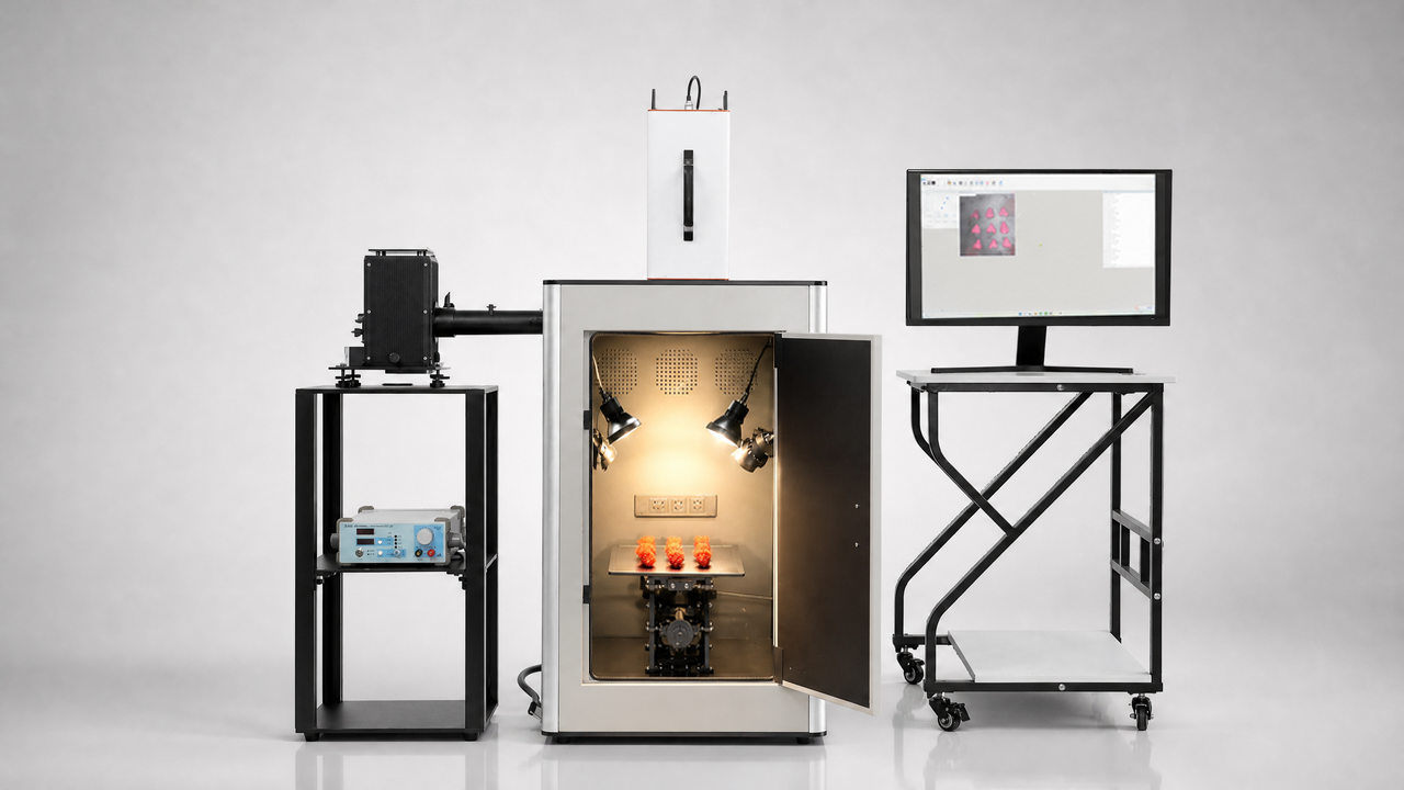
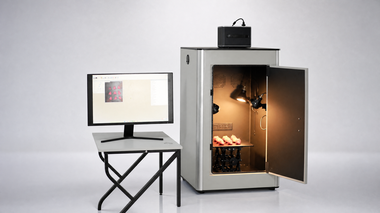
设备:GaiaField
Origins of Inhomogeneous Light Emission From GaN-Based Flip-Chip GreenMicro-LEDs
Abstract:Spatially resolved electroluminescence emit ted through the sapphire substrate of GaN-based flip-chip green microscale light-emitting diodes with 20 × 20 μm2 mesas has been collected via microscopic hyperspectral imaging. The current crowding is identified in the central region of the mesa, corresponding to the position of the p-pad. The bright-spot emissions at the edges of the mesa originate from localized potential energy valleys . This letter suggests that the comprehensive information about current crowding and the distribution of the light emission across the mesa of microscale light-emitting diode can be obtained by capturing spatially resolved light emission from the side of the transparent substrate.
Index Terms:Micro-LEDs, current crowding, spatially resolved electroluminescence.